
Copper foil is a critical material in various industries, including electronics, automotive, and energy storage, particularly in the production of printed circuit boards (PCBs) and lithium-ion batteries. The quality of copper foil directly impacts the performance and reliability of the final products. As such, detecting and addressing defects in copper foil during the manufacturing process is essential to ensure high standards of quality and efficiency. This article explores the importance of copper foil defect detection, common types of defects, and the technologies used to identify and mitigate these issues.
Importance of Copper Foil Defect Detection
Copper foil defects can lead to significant problems in the performance of electronic devices. For instance, in PCBs, even minor imperfections can cause short circuits, signal interference, or complete failure of the circuit. In lithium-ion batteries, defects in the copper foil used as a current collector can affect the battery's efficiency, lifespan, and safety. Therefore, early detection of defects is crucial to prevent costly recalls, ensure product reliability, and maintain customer trust.
Common Types of Copper Foil Defects
-
Surface Scratches and Dents: These are often caused by mechanical handling or improper storage. Scratches can affect the uniformity of the foil, leading to issues in subsequent processing steps such as etching or plating.
-
Pinholes: Tiny holes in the copper foil can result from impurities in the raw material or during the manufacturing process. Pinholes can compromise the structural integrity of the foil and lead to failures in the final product.
-
Oxidation and Corrosion: Exposure to moisture or corrosive environments can cause oxidation or corrosion on the copper surface. This not only affects the appearance but also the electrical conductivity of the foil.
-
Thickness Variations: Inconsistent thickness across the foil can lead to uneven current distribution in electronic applications, affecting performance and reliability.
-
Contamination: Foreign particles or residues on the surface can interfere with the adhesion of subsequent layers or coatings, leading to delamination or poor electrical contact.
Technologies for Copper Foil Defect Detection
Advancements in technology have led to the development of sophisticated methods for detecting defects in copper foil. These methods leverage automation, machine learning, and high-resolution imaging to ensure accurate and efficient detection.
-
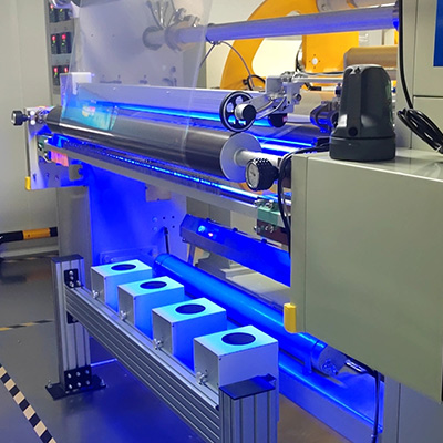
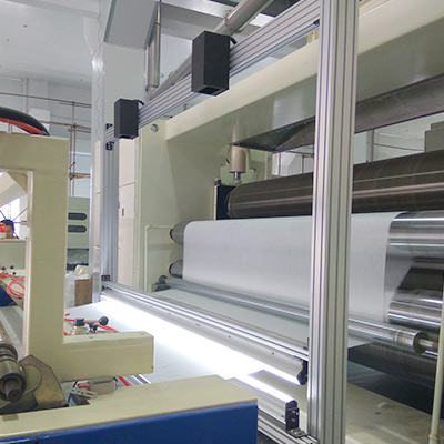
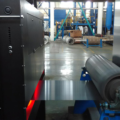
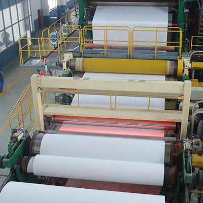
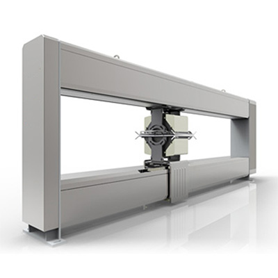
Automated Optical Inspection (AOI): AOI systems use high-resolution cameras and advanced image processing algorithms to scan the surface of the copper foil. These systems can detect a wide range of defects, including scratches, pinholes, and contamination, with high precision. AOI is widely used in the PCB industry for its ability to provide real-time feedback and integrate seamlessly into production lines.
-
Laser Scanning: Laser-based systems can measure the thickness and surface topography of the copper foil with high accuracy. By analyzing the reflected laser light, these systems can identify variations in thickness and detect surface irregularities that may not be visible to the naked eye.
-
Eddy Current Testing: This non-destructive testing method uses electromagnetic induction to detect surface and near-surface defects in conductive materials like copper. Eddy current testing is particularly effective for identifying cracks, pinholes, and other subsurface defects that may not be detectable through visual inspection.
-
Machine Learning and AI: Machine learning algorithms can be trained to recognize patterns associated with various types of defects. By analyzing large datasets of images and sensor data, AI systems can improve defect detection accuracy over time and adapt to new types of defects. This approach is increasingly being integrated into AOI and other inspection systems to enhance their capabilities.
-
X-ray Inspection: X-ray systems can penetrate the copper foil to detect internal defects such as voids, inclusions, or delaminations. This method is particularly useful for inspecting thicker foils or multi-layer structures where surface inspection methods may not be sufficient.
Benefits of Advanced Defect Detection
Implementing advanced defect detection technologies offers several benefits:
-
Improved Product Quality: Early detection and removal of defective foil ensures that only high-quality material is used in the final product, enhancing performance and reliability.
-
Reduced Waste: By identifying defects early in the production process, manufacturers can minimize material waste and reduce costs associated with rework or scrap.
-
Increased Efficiency: Automated inspection systems can operate at high speeds, allowing for continuous monitoring without slowing down production lines.
-
Enhanced Safety: Detecting defects that could lead to failures in critical applications, such as batteries or electronic devices, helps prevent potential safety hazards.

Conclusion
Copper foil defect detection is a vital aspect of modern manufacturing, particularly in industries where precision and reliability are paramount. By leveraging advanced technologies such as AOI, laser scanning, eddy current testing, and AI-driven systems, manufacturers can ensure the highest standards of quality while improving efficiency and reducing costs. As the demand for high-performance electronic devices and energy storage solutions continues to grow, the importance of effective defect detection in copper foil production will only increase, driving further innovation in this field.


 Top
Top
 Email
Email
 WhatsApp

 Submit Form
 Down
Down